- 您现在的位置:买卖IC网 > Sheet目录492 > NTMSD3P303R2G (ON Semiconductor)MOSFET P-CH 30V 2.34A 8-SOIC
�� �
�
�NTMSD3P303R2�
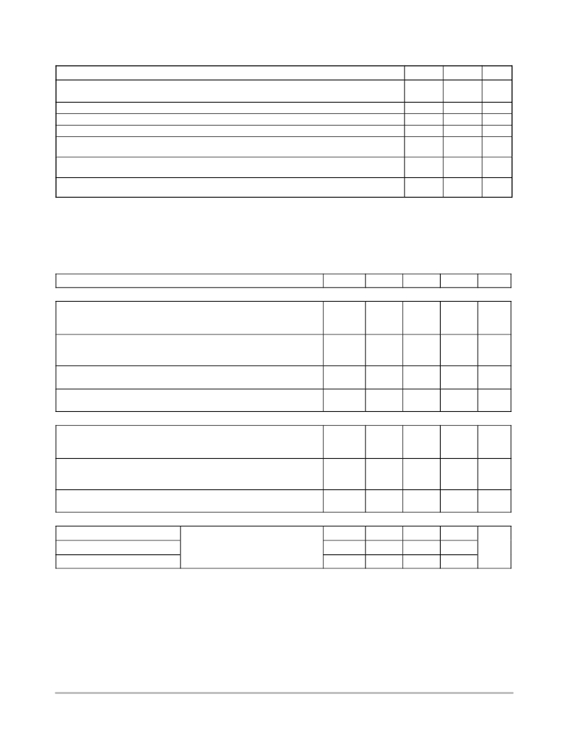
�SCHOTTKY� MAXIMUM� RATINGS� (T� J� =� 25� °� C� unless� otherwise� noted)�
�Rating�
�Peak� Repetitive� Reverse� Voltage�
�DC� Blocking� Voltage�
�Thermal� Resistance� ?� Junction� ?� to� ?� Ambient� (Note� 5)�
�Thermal� Resistance� ?� Junction� ?� to� ?� Ambient� (Note� 6)�
�Thermal� Resistance� ?� Junction� ?� to� ?� Ambient� (Note� 7)�
�Average� Forward� Current� (Note� 7)�
�(Rated� V� R� ,� T� A� =� 100� °� C)�
�Peak� Repetitive� Forward� Current� (Note� 7)�
�(Rated� V� R� ,� Square� Wave,� 20� kHz,� T� A� =� 105� °� C)�
�Non� ?� Repetitive� Peak� Surge� Current� (Note� 7)�
�(Surge� Applied� at� Rated� Load� Conditions,� Half� ?� Wave,� Single� Phase,� 60� Hz)�
�Symbol�
�V� RRM�
�V� R�
�R� q� JA�
�R� q� JA�
�R� q� JA�
�I� O�
�I� FRM�
�I� FSM�
�Value�
�30�
�197�
�97�
�62.5�
�3.0�
�6.0�
�30�
�Unit�
�V�
�°� C/W�
�°� C/W�
�°� C/W�
�A�
�A�
�A�
�Stresses� exceeding� Maximum� Ratings� may� damage� the� device.� Maximum� Ratings� are� stress� ratings� only.� Functional� operation� above� the�
�Recommended� Operating� Conditions� is� not� implied.� Extended� exposure� to� stresses� above� the� Recommended� Operating� Conditions� may� affect�
�device� reliability.�
�5.� Minimum� FR� ?� 4� or� G� ?� 10� PCB,� Steady� State.�
�6.� Mounted� onto� a� 2� ″� square� FR� ?� 4� Board� (1� in� sq,� 2� oz� Cu� 0.06� ″� thick� single� sided),� Steady� State.�
�7.� Mounted� onto� a� 2� ″� square� FR� ?� 4� Board� (1� in� sq,� 2� oz� Cu� 0.06� ″� thick� single� sided),� t� ≤� 10� seconds.�
�ELECTRICAL CHARACTERISTICS� (T� J� = 25� °� C unless otherwise noted) (No� te� 8)�
�Characteristic�
�Symbol�
�Min�
�Typ�
�Max�
�Unit�
�OFF� CHARACTERISTICS�
�Drain� ?� to� ?� Source� Breakdown� Voltage�
�(V� GS� =� 0� Vdc,� I� D� =� ?� 250� m� Adc)�
�Temperature� Coefficient� (Positive)�
�Zero� Gate� Voltage� Drain� Current�
�(V� DS� =� ?� 30� Vdc,� V� GS� =� 0� Vdc,� T� J� =� 25� °� C)�
�(V� DS� =� ?� 30� Vdc,� V� GS� =� 0� Vdc,� T� J� =� 125� °� C)�
�Gate� ?� Body� Leakage� Current�
�(V� GS� =� ?� 20� Vdc,� V� DS� =� 0� Vdc)�
�Gate� ?� Body� Leakage� Current�
�(V� GS� =� +20� Vdc,� V� DS� =� 0� Vdc)�
�V� (BR)DSS�
�I� DSS�
�I� GSS�
�I� GSS�
�?� 30�
�?�
�?�
�?�
�?�
�?�
�?�
�?� 30�
�?�
�?�
�?�
�?�
�?�
�?�
�?� 1.0�
�?� 25�
�?� 100�
�100�
�Vdc�
�mV/� °� C�
�m� Adc�
�nAdc�
�nAdc�
�ON� CHARACTERISTICS�
�Gate� Threshold� Voltage�
�(V� DS� =� V� GS� ,� I� D� =� ?� 250� m� Adc)�
�Temperature� Coefficient� (Negative)�
�Static� Drain� ?� to� ?� Source� On� ?� State� Resistance�
�(V� GS� =� ?� 10� Vdc,� I� D� =� ?� 3.05� Adc)�
�(V� GS� =� ?� 4.5� Vdc,� I� D� =� ?� 1.5� Adc)�
�Forward� Transconductance�
�(V� DS� =� ?� 15� Vdc,� I� D� =� ?� 3.05� Adc)�
�V� GS(th)�
�R� DS(on)�
�g� FS�
�?� 1.0�
�?�
�?�
�?�
�?�
�?� 1.7�
�3.6�
�0.063�
�0.090�
�5.0�
�?� 2.5�
�?�
�0.085�
�0.125�
�?�
�Vdc�
�W�
�Mhos�
�DYNAMIC� CHARACTERISTICS�
�Input� Capacitance�
�Output� Capacitance�
�Reverse� Transfer� Capacitance�
�(V� DS� =� ?� 24� Vdc,�
�V� GS� =� 0� Vdc,�
�f� =� 1.0� MHz)�
�C� iss�
�C� oss�
�C� rss�
�?�
�?�
�?�
�520�
�170�
�70�
�750�
�325�
�135�
�pF�
�8.� Handling� precautions� to� protect� against� electrostatic� discharge� are� mandatory.�
�http://onsemi.com�
�2�
�发布紧急采购,3分钟左右您将得到回复。
相关PDF资料
NTMSD6N303R2G
MOSFET N-CH 30V 6A 8-SOIC
NTNUS3171PZT5G
MOSFET P-CH 20V 200MA SOT-1123
NTP125N02RG
MOSFET N-CH 24V 15.9A TO220AB
NTP18N06G
MOSFET N-CH 60V 15A TO220AB
NTP18N06LG
MOSFET N-CH 60V 15A TO220AB
NTP2955
MOSFET P-CH 60V 2.4A TO220AB
NTP30N06LG
MOSFET N-CH 60V 30A TO220AB
NTP30N20G
MOSFET N-CH 200V 30A TO220AB
相关代理商/技术参数
NTMSD6N303
制造商:ONSEMI 制造商全称:ON Semiconductor 功能描述:Typical Uses for FETKY Devices
NTMSD6N303R2
功能描述:MOSFET 30V 6A N-Channel RoHS:否 制造商:STMicroelectronics 晶体管极性:N-Channel 汲极/源极击穿电压:650 V 闸/源击穿电压:25 V 漏极连续电流:130 A 电阻汲极/源极 RDS(导通):0.014 Ohms 配置:Single 最大工作温度: 安装风格:Through Hole 封装 / 箱体:Max247 封装:Tube
NTMSD6N303R2G
功能描述:MOSFET 30V 6A N-Channel RoHS:否 制造商:STMicroelectronics 晶体管极性:N-Channel 汲极/源极击穿电压:650 V 闸/源击穿电压:25 V 漏极连续电流:130 A 电阻汲极/源极 RDS(导通):0.014 Ohms 配置:Single 最大工作温度: 安装风格:Through Hole 封装 / 箱体:Max247 封装:Tube
NTMSD6N303R2SG
功能描述:MOSFET NFET 30V 6A .024R RoHS:否 制造商:STMicroelectronics 晶体管极性:N-Channel 汲极/源极击穿电压:650 V 闸/源击穿电压:25 V 漏极连续电流:130 A 电阻汲极/源极 RDS(导通):0.014 Ohms 配置:Single 最大工作温度: 安装风格:Through Hole 封装 / 箱体:Max247 封装:Tube
NTN12
制造商:OTAX Corporation 功能描述:
NTN22
制造商:OTAX Corporation 功能描述:Tape & Reel
NTN32
制造商:OTAX Corporation 功能描述:
NTN4327A
制造商:Dantona Industries 功能描述:NICKEL CADMIUM BATTERY, 7.5V, 1.8AH; Battery Capacity:1.8Ah; Battery Voltage:7.5V; Battery Technology:Nickel Cadmium; External Height:94.996mm; External Width:69.596mm; External Depth:35.56mm; Battery Terminals:Pressure Contact ;RoHS Compliant: NA